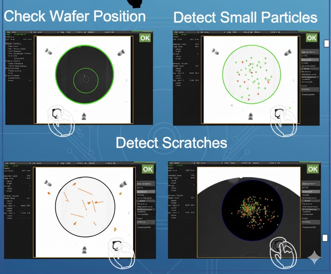
Key Features
- High-Resolution Imaging: Sub-nanometer sensitivity for detecting particles, pattern defects, scratches, and overlay errors.
- AI-Based Classification: Machine learning models automatically categorize defect types and severities for faster root cause analysis.
- Inline & Offline Inspection: Flexible deployment for wafer, mask, and packaging defect detection.
- Yield Enhancement: Provides actionable data to optimize process parameters and reduce defect density.
- Scalable Coverage: Compatible with 200mm and 300mm wafers, across lithography, etch, deposition, CMP, and assembly lines.
- Smart Integration: Connects seamlessly with MES, FDC, and predictive maintenance platforms for fab-wide defect tracking.
Value Proposition
The Defect Detection System safeguards semiconductor yield by enabling early, accurate, and automated defect identification. With faster turnaround and higher precision, it helps fabs minimize scrap, optimize processes, and accelerate time-to-market in advanced nodes and legacy production alike.